Complutense University of Madrid | UCM
About
The Complutense University of Madrid, with nearly 80,000 students, is the largest classroom learning university in Spain, one of the most prestigious in Europe, and a centre of reference for Latin America.

Group for the Physics of Complex Materials
Founded in 1499 under Cardinal Cisneros, the Complutense University of Madrid (UCM)is a historic institution and a global leader in research, renowned for its contributions to fields such as science, humanities, engineering, and health. With over 90,000 students and 170 master’s programs, UCM blends academic tradition with innovation, ranking as the third-largest on-campus university in Europe
The GFMC (Group for the Physics of Complex Materials) research group belongs to the Department of Materials Physics at the UCM Physics Faculty. The group is devoted to the fabrication (epitaxial growth) and characterization of thin films, nanostructures and heterostructures of correlated oxides with special emphasis on magnetism and superconductivity and ion diffusion in solids. The group has longstanding experience on the research topic of the proposal, in particular, on the fabrication of planar and vertical oxide nanostructures based on correlated oxides for non-equilibrium spin transport (ferroelectric tunnel junctions, superconductor spintronics and spin orbitronics). In the last 20 years the group has made significant advances on the physics of complex oxides interfaces
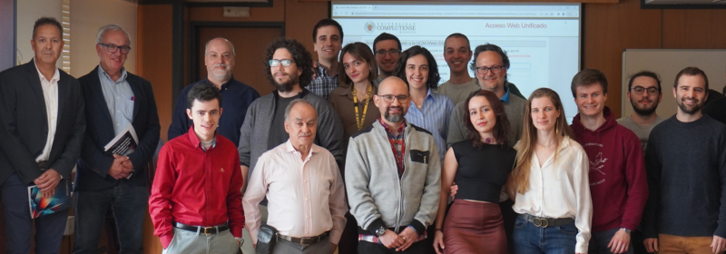
Our team
Jacobo Santamaria (PI)
Carlos Leon (Research scientist)
David Sanchez-Manzano (Research scientist)
Lab tour
Epitaxial growth of oxide materials
We produce films and heterostructures combining very different materials including YBa2Cu3O7, La0.7Sr0.3 MnO3, BaTiO3 , SrRuO3 , SrIrO3 , NdNiO3.
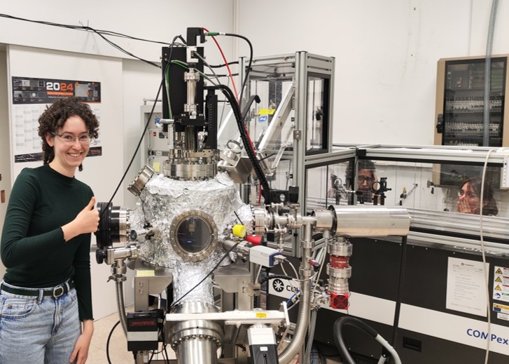
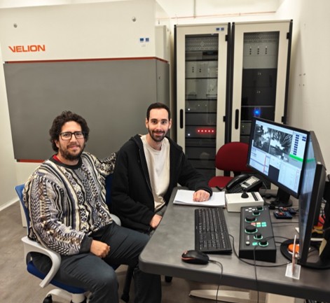
Pulsed Laser Deposition (PLD) with Reflection High-Energy Electron Diffraction (RHEED) system to monitor the layer-by-layer grow of oxide films.
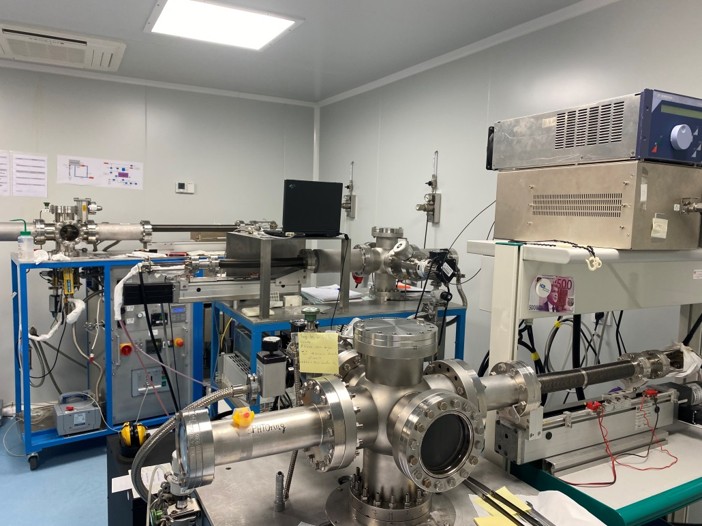
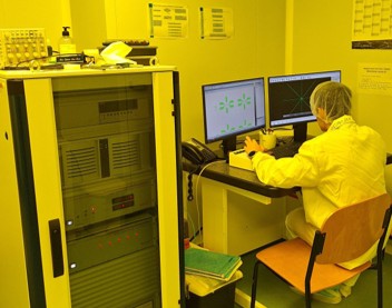
High temperature (<1000 ºC) pure oxygen high pressure (3 mbar) sputtering systems installed in a clean room environment. Targets (up to 5) are mounted on a mobile arm to enable switching growth between different materials. This technique is optimized for the growth of High Tc Superconductors.
Fabrication of oxide nanostructures
We combine different nanofabrication tools to engineer planar and vertical junctions to measure charge and spin transport
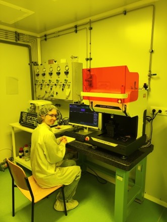
Respectively: 1) Projection UV lithography system for maskless device definition (~1µm) 2) Electron Beam Lithography (EBL) system with ~100nm spatial resolution 3) Dual beam (electronic-ionic) for 3D lithography with (~10nm) for high precision fabrication of oxide devices